

Intel Unveils Cutting-Edge Packaging Power: 16 Compute Tiles and 24 HBM Sites with Advanced 3D Tech
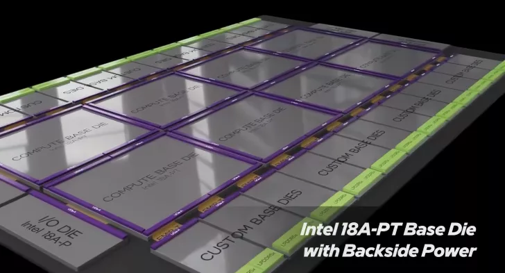
Intel is making waves in the semiconductor industry with its latest advancements in chip packaging technology. The company has unveiled a new multi-chiplet product that utilizes the 18A and 14A process nodes, along with cutting-edge Foveros 3D and EMIB-T technologies. These innovations promise to set new standards in computing for high-performance computing, AI, and data centers.
Intel’s Next-Gen Innovations: A Technological Leap
Intel is not holding back in showcasing its advanced packaging solutions, paving the way for the next generation of chips. The new technologies aim to rival TSMC’s CoWoS solutions, positioning Intel as a formidable competitor. With up to 16 compute tiles and 24 HBM sites, Intel’s designs offer scalable solutions for a variety of applications.
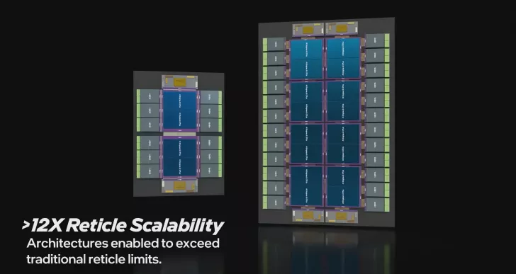
These designs are integrated with EMIB-T interconnect for superior bandwidth, allowing the use of both current and future HBM standards. Intel’s advanced package can accommodate up to 48 LPDDR5x controllers, making it highly suitable for AI and data center workloads.
Engagement with Industry Partners
Intel’s diverse ecosystem engagement plan involves working closely with industry partners to accelerate time-to-market and enhance supply chain resilience. The company is actively seeking collaborations with new customers, particularly with its 14A node, designed for third-party use.
The future holds promise as Intel continues to innovate with projects like Jaguar Shores and the Crescent Island GPU for AI. However, much depends on securing deals for its 14A technology, which is crucial for Intel’s competitive standing in the semiconductor industry.