NVIDIA Takes the Lead: Exclusive Customer of TSMC’s Cutting-Edge A16 Process for Future GPUs
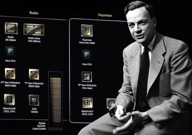
NVIDIA is setting its sights on the cutting-edge A16 process technology from TSMC for its future Feynman GPUs. As the demand for advanced chips continues to rise in the AI sector, NVIDIA is not only enhancing its current Blackwell Ultra chips but also urging TSMC to accelerate its P3 plant operations. This plant is expected to play a crucial role in mass-producing the upcoming Rubin chips, which will utilize TSMC’s 3nm process technology, marking a significant leap forward from the 4NP technology used in Blackwell Ultra chips.
NVIDIA’s Strategic Move with TSMC’s A16 Technology
According to recent reports, NVIDIA stands as the sole customer for TSMC’s A16 technology, which promises to be the backbone for their next-gen GPUs, succeeding the Rubin 2026 and Rubin Ultra 2027 series. This strategic positioning aligns with NVIDIA’s ambitious roadmap for AI advancements and the introduction of Vera Rubin Superchips, anticipated for production by 2026 and potentially available by Q3 of the same year.

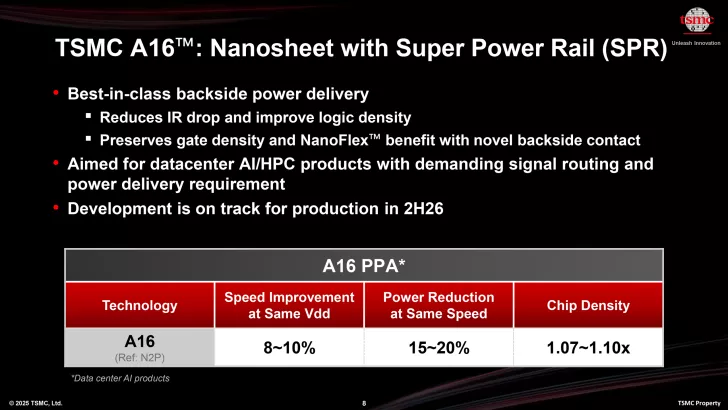
NVIDIA will be the exclusive debut user of TSMC’s A16 process, which will be crucial for the Feynman GPUs. As mass production is slated to begin in 2027, this move will significantly impact NVIDIA’s product development and market competition. The A16 node, with its speed boost and power efficiency, represents a significant upgrade from the current N3P tech.
The Future Landscape for NVIDIA in AI
As NVIDIA continues to dominate the AI sector, the expansion of 3nm capacity by TSMC is a response to the large orders from NVIDIA, further reinforcing their collaboration. The A16 process is set to utilize innovative nanosheet technology with SPR, enhancing power delivery specifically for AI and HPC applications, and is expected to be ready for production by late 2026.

The relationship between NVIDIA and TSMC continues to flourish, recently marked by the production of the first Blackwell wafer on US soil. This collaboration is expected to further intensify as they address AI market demands, even as competitors like AMD, Microsoft, and Google gear up for the challenge.
NVIDIA Data Center / AI GPU Roadmap
| GPU Codename | Feynman | Rubin (Ultra) | Rubin | Blackwell (Ultra) | Blackwell | Hopper | Ampere | Volta | Pascal |
|---|---|---|---|---|---|---|---|---|---|
| GPU Family | GF200? | GR300? | GR200? | GB300 | GB200/GB100 | GH200/GH100 | GA100 | GV100 | GP100 |
| GPU SKU | F200? | R300? | R200? | B300 | B100/B200 | H100/H200 | A100 | V100 | P100 |
| Process Tech | TSMC A16? | TSMC N2P? | TSMC N3P? | TSMC 4NP | TSMC 4NP | TSMC 5nm | TSMC 7nm | TSMC 12nm | TSMC 16nm |
| Memory | HBM4e/HBM5? | HBM4 | HBM4 | HBM3e | HBM3e | HBM2e/HBM3/HBM3e | HBM2e | HBM2 | HBM2 |
| Launch | 2028 | 2027 | 2026 | 2025 | 2024 | 2022-2024 | 2020-2022 | 2018 | 2016 |