Amidst the growing demand for advanced packaging solutions, TSMC is setting its sights on transforming an Arizona fab site into a cutting-edge packaging facility. This move is aimed at catering to the increasing requirements of U.S. clients, particularly in the realms of AI GPUs and ASICs. With companies like NVIDIA and AMD prioritizing U.S. production, the absence of TSMC’s advanced packaging capabilities locally has pushed these tech giants to explore other avenues, including competitors. However, TSMC seems poised to address these challenges and meet the burgeoning demand.
TSMC’s Strategic Expansion in Arizona
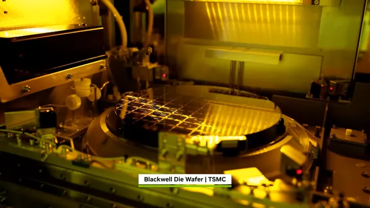
The Taiwan-based tech giant is reportedly expediting its plans to introduce advanced packaging lines in the United States. By converting a portion of the Arizona fab reserved for chip fabrication into a packaging facility, TSMC aims to alleviate the pressing need for local packaging technologies. This strategic shift comes as U.S.-produced wafers, such as NVIDIA’s Blackwell, have been sent to Taiwan for final processing. Previously, TSMC relied on outsourcing these services to American firms like Amkor, but this approach is now undergoing a significant transformation.

Competition and Industry Dynamics
Due to current supply constraints, U.S. customers, including Microsoft, Qualcomm, Apple, and Tesla, are turning to competitors such as Intel, adopting their EMIB and Foveros technologies as alternatives. This growing interest in Intel’s solutions has likely influenced TSMC’s decision to fast-track its plans for an Arizona-based packaging facility. The new facility is expected to play a crucial role in addressing a substantial portion of the U.S. industry’s chip demand.
As TSMC’s project in Arizona progresses, it will be fascinating to observe how this development impacts the local market and the broader technology landscape.
